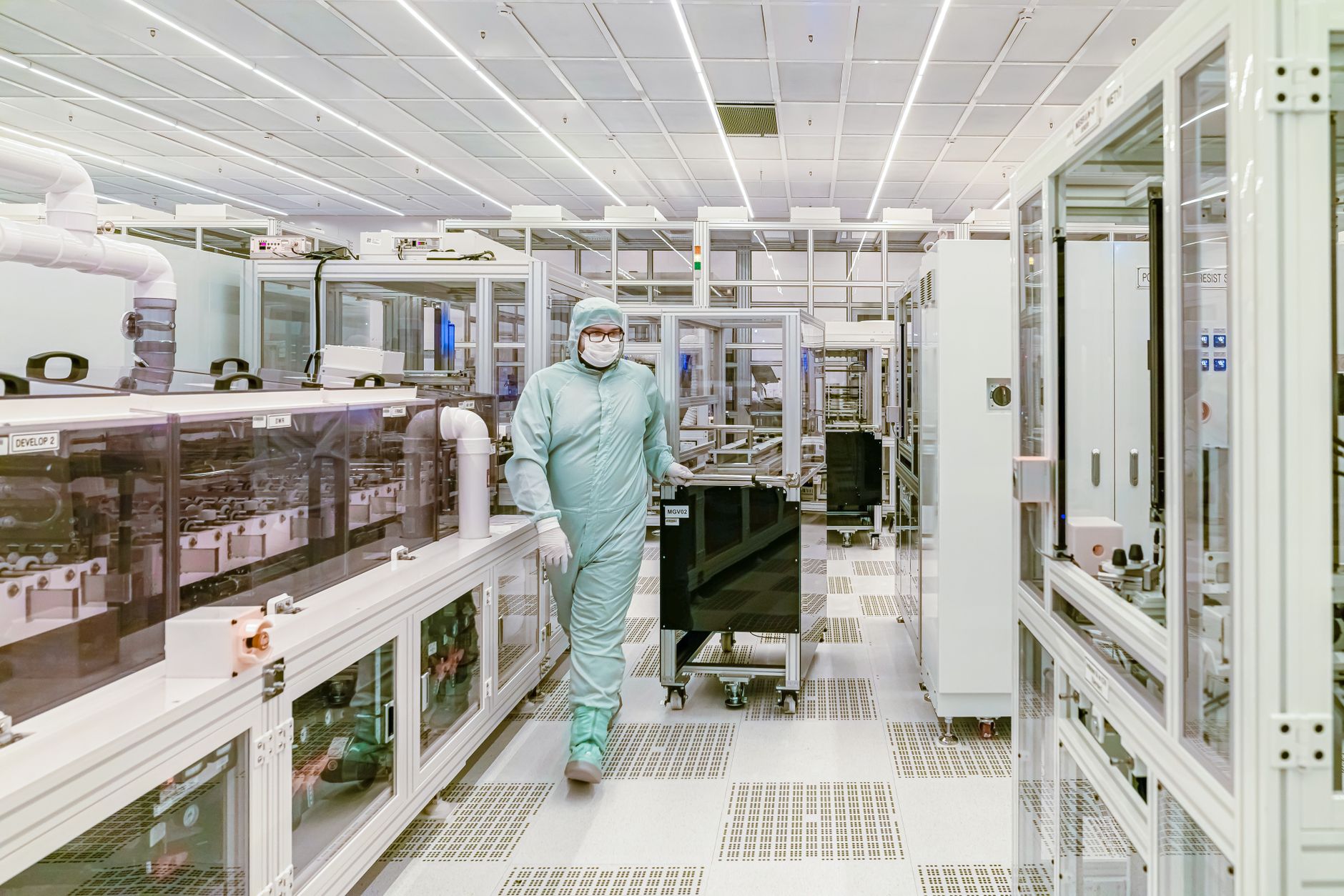
The Dholera semiconductor fab is India's first commercial-scale chip fabrication plant, being built by Tata Electronics in partnership with Taiwan's Powerchip Semiconductor Manufacturing Corp (PSMC). The Union Cabinet approved it on 29 February 2024 under the India Semiconductor Mission, with a stated investment of about Rs 91,000 crore (roughly US$11 billion). The plant is designed for up to 50,000 wafers a month on 300mm wafers, using mature and specialty nodes of 28, 40, 55, 90 and 110 nm. Ground was broken in March 2024, civil work was reported at around 50 percent by May 2026, and an ASML lithography MoU was signed on 17 May 2026. A first chip is targeted for 2026-27, but no source confirms a chip has been produced yet, so that date is a target, not a fact.
The Dholera semiconductor fab is India's first commercial-scale chip fabrication plant, built by Tata Electronics with Taiwan's Powerchip Semiconductor Manufacturing Corp, known as PSMC. The Union Cabinet cleared it on 29 February 2024 under the India Semiconductor Mission, at a stated investment of about Rs 91,000 crore, or roughly US$11 billion. This page sets out what is confirmed, what is under construction, and what remains a target, using dated figures only. Where a claim is a projection rather than a done deal, it is flagged plainly.
The short answer
A semiconductor fab, short for fabrication plant, is a factory that turns silicon wafers into finished chips. The Dholera fab is being developed by Tata Semiconductor Manufacturing Pvt Ltd, a Tata Electronics entity, in partnership with PSMC, which brings process technology. It is the anchor industrial project of the Dholera Special Investment Region and one of the reasons the region is described as India's coming chip hub. Importantly, this is a separate, approved project and should not be confused with the earlier collapsed plan covered in our Vedanta-Foxconn history.
Who is building it
The plant is owned and run through Tata Semiconductor Manufacturing Pvt Ltd, the fab arm of Tata Electronics. The technology partner is Powerchip Semiconductor Manufacturing Corp of Taiwan, a foundry that supplies proven process recipes and manufacturing know-how. This split is common for a country building its first fab: the local group supplies capital, land, and long-term ownership, while the foreign partner supplies the process technology that takes years to develop in-house.
The India Semiconductor Mission, or ISM, is the central government programme that makes the economics work. For this project, ISM support covers 50 percent of the eligible project cost. The formal Fiscal Support Agreement was signed on 5 March 2025, roughly a year after Cabinet approval, which is the step that locked in the government's financial commitment.
Investment, capacity, and what it will make
The headline number is a stated investment of about Rs 91,000 crore. The Press Information Bureau, in the Fiscal Support Agreement, cites a more precise Rs 91,526 crore. In US dollar terms this is usually reported as around US$11 billion. The plant is a 300mm wafer fab, the standard large-wafer format for high-volume production, with a target capacity of up to 50,000 wafers per month once fully ramped.
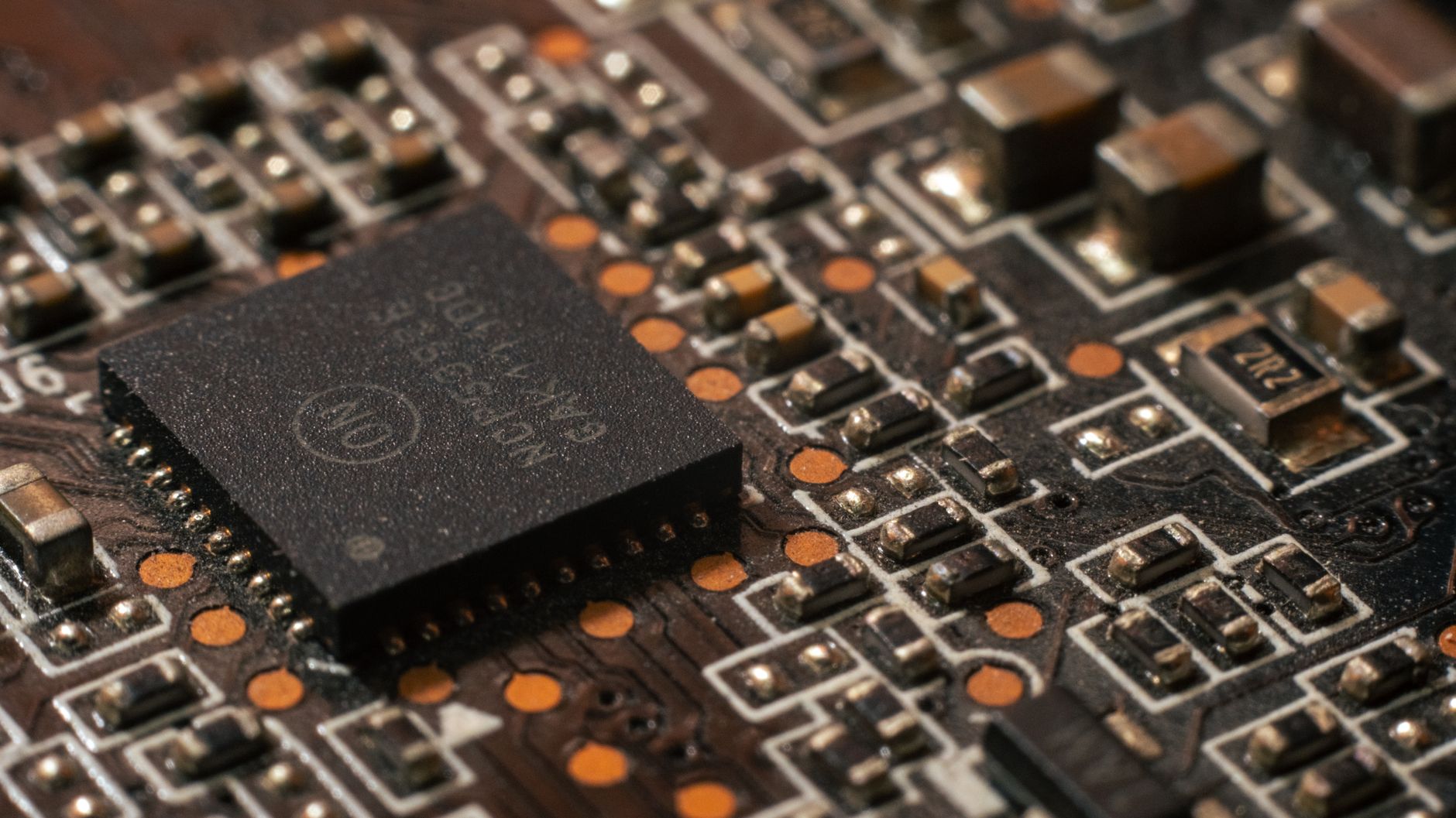
The fab targets mature and specialty process nodes rather than the bleeding edge. The stated nodes are 28, 40, 55, 90 and 110 nm. These are the workhorse geometries used across power-management chips, display driver ICs, microcontrollers, and high-performance-computing logic. This is a deliberate strategy: mature nodes have huge, durable demand across cars, appliances, phones, and industrial gear, and they are where a first-time national fab can compete without chasing the most expensive frontier processes.
| Specification | Figure | Status |
|---|---|---|
| Cabinet approval | 29 February 2024 | Confirmed |
| Stated investment | ~Rs 91,000 cr (PIB cites Rs 91,526 cr) | Confirmed approval figure |
| ISM fiscal support | 50% of eligible cost | Confirmed |
| Fiscal Support Agreement | Signed 5 March 2025 | Confirmed |
| Wafer size | 300mm | Confirmed |
| Target capacity | Up to 50,000 wafers per month | Target, at full ramp |
| Process nodes | 28 / 40 / 55 / 90 / 110 nm | Confirmed plan |
| Ground-breaking | March 2024 | Confirmed |
| Civil progress | ~50% complete | Reported, May 2026 |
| ASML lithography MoU | 17 May 2026 | Confirmed |
| First chip | 2026-27 | Target, not confirmed produced |
The construction timeline
The project has moved through a clear sequence of dated milestones. Ground was broken in March 2024, soon after Cabinet approval. Through late 2025 the site was reportedly redesigned to suit local soil conditions, which is a normal engineering step for a heavy, vibration-sensitive facility on coastal ground. By May 2026, civil work was reported at around 50 percent complete.
A significant supply-chain milestone came on 17 May 2026, when Tata signed a memorandum of understanding with ASML, the Dutch company that makes the lithography systems at the heart of any fab. Lithography is the step that prints circuit patterns onto wafers, so securing that relationship is a meaningful marker of intent. A first chip out of the line is targeted for 2026-27. As of this page's date, no source confirms that a chip has actually been produced, so treat 2026-27 as a target date, not an achievement.
Jobs and the wider economic case
Employment figures for the fab are stated as targets. The project is associated with more than 20,000 direct and indirect jobs, and a broader multi-fab vision for the region has referenced around 100,000 jobs over the long run. Both are targets tied to full build-out and future expansion, not current headcount. The value of a fab, though, is not only its own payroll. Chip plants pull in a dense supplier ecosystem of gases, chemicals, tooling, and services, and they tend to anchor other advanced manufacturing nearby, which is exactly the effect Dholera's planners want across the region's planned industrial sectors.
The fab also explains why other regional infrastructure exists in the form it does. A fab needs enormous, uninterrupted, clean power and large volumes of ultra-pure water, which is part of the logic behind the region's solar park and its heavy investment in trunk utilities. The chip plant, the power, and the water systems are best read as parts of one industrial-city design.
How this differs from the collapsed Vedanta-Foxconn plan
Many readers arrive here searching for "Vedanta semiconductor" because an earlier, much-publicised Dholera-linked chip plan involved Vedanta and Foxconn. That joint venture, announced in September 2022, never built a plant; Foxconn withdrew in July 2023 and the venture dissolved. The Tata and PSMC fab is a separate, later, Cabinet-approved project that is actually under construction. The two are unrelated in ownership and status. For the full story of the earlier plan and why it collapsed, see our Vedanta-Foxconn history.
Frequently asked questions
Who is building the Dholera semiconductor fab?
How much is the Dholera fab costing?
What chips will the Dholera fab make?
Has the Dholera fab produced a chip yet?
Is this the same as the Vedanta-Foxconn project?
How many jobs will the Dholera fab create?
DholeraPulse. (2026). Dholera Semiconductor Fab: Tata Electronics and PSMC, Explained. Retrieved 22 July 2026, from https://dholerapulse.com/dholera-semiconductor-fabSources & references
- Dholerapedia Fact Pack (verified July 2026)
- Press Information Bureau, PRID 2108602 (India Semiconductor Mission, Tata fab approval and Fiscal Support Agreement)
- Tata Electronics and tataelectronics.com (TEPL-PSMC fab details)
- Tom's Hardware (ASML-Tata lithography MoU, 2026)
- Union Cabinet approval announcement, 29 February 2024
DholeraPulse labels facts by confidence. Figures marked reported or target come from press or announcements and may change; verify anything time sensitive against the official source before acting.